DESIGN, PACKAGING AND CHARACTERISATION OF PHOTONIC INTEGRATED CIRCUITS: THE FIRST EDITION OF PHOTONICS COURSES STARTS AT THE TECIP INSTITUTE
The first edition, tuition free, of the first module of "Photonic Integrated Circuits Design, Fabrication & Packaging" organized by the Photonics Integrated Technologies Center INPHOTEC of the Institute of Communication, Information and Perception Technologies (TeCIP) of Scuola Superiore Sant'Anna, in collaboration with the National Inter-University Consortium for Telecommunications (CNIT) will be held from 5 to 15 September.
This first meeting covers one module of 3-module course, for a total duration of 4 weeks program, which can also be attended individually, and is aimed at strengthening skills in the design, fabrication and packaging of photonic integrated circuits.
For the entire duration of the event the TeCIP Institute opens the doors of its classrooms and its laboratories to all selected candidates both from academic and industrial fields and, at the same time, professionals with an adequate background willing to develop specific and comprehensive skills upon design, fabrication, packaging and characterization of photonic integrated circuits.
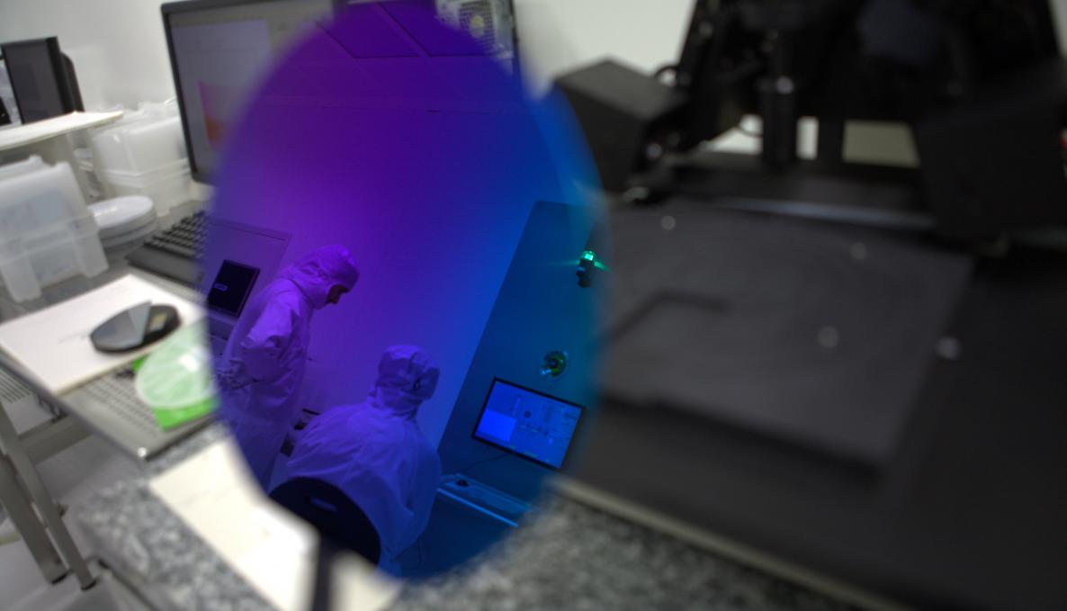
Participating in this extraordinary event gives us all a great opportunity to focus on strategic issues and, through lectures and laboratory exercises, to interact with a unique infrastructure in Italy - the Clean Room - which operates in a highly strategic environment oriented towards design sessions within the front-end (fabrication) and back-end (packaging) infrastructures.
Lectures by Dr. RemcoStoffer and Dr. Luis Orbe of PhoeniX Software have been scheduled to make the event even more international. A closer working relationship with the Dutch company has been established to find most advanced solutions in photonic integrated circuits design and manufacturing.
The Integrated Photonic Technologies Center of the Sant’Anna School of Advanced Studies of Pisa has been fully operational since 1st January 2015, created with a contribution provided by the Regione Toscana. 700 square meters are dedicated to clean rooms and it has four technological platforms: Silicon Photonics, Glass in Silicon, Hybrid Integration and Advanced Packaging.
Next events will be the Photonic Integrated Circuit Design and Fabrication (PIC D & F) from 14 to 18 November 2016 and Characterization and Testing (C & T) Session from 20 to 24 March 2017.
More on INPHOTEC and TeCIP Institute on this video.
For further details, please find attached the meeting brochure.